
The escalating capabilities of quantum computing present an existential threat to contemporary cryptographic protocols, necessitating a paradigm shift in secure communication. Quantum cryptography, which leverages the fundamental principles of quantum mechanics, offers a robust alternative by ensuring data security through physical laws rather than computational complexity. However, the widespread adoption of quantum communication hinges on the development of miniaturized, highly stable, and cost-effective devices capable of accurately manipulating and detecting the exceedingly delicate quantum signals encoded in light. Recent advancements demonstrate a significant leap forward in this domain, utilizing an unexpected yet profoundly suitable material: borosilicate glass, meticulously transformed into sophisticated photonic integrated circuits through ultrafast laser technology.
The Quantum Imperative: A Looming Threat and a Foundational Solution
The advent of quantum computing heralds a new era of computational power, promising to revolutionize fields from medicine to materials science. Concurrently, it poses a profound challenge to global cybersecurity infrastructure. Algorithms like Shor’s algorithm, for instance, are theoretically capable of efficiently factoring large prime numbers, the mathematical bedrock of widely used public-key encryption schemes such as RSA and elliptic curve cryptography (ECC). Similarly, Grover’s algorithm could significantly accelerate brute-force attacks on symmetric key ciphers. This "quantum threat" mandates a proactive development of post-quantum cryptographic solutions that can withstand the computational prowess of future quantum machines.
Quantum cryptography emerges as a leading contender in this race, offering an intrinsically secure communication paradigm. Unlike classical cryptography, which relies on computational hardness assumptions, quantum cryptography derives its security from immutable laws of physics, such as the Heisenberg Uncertainty Principle and the no-cloning theorem. These principles fundamentally prevent an eavesdropper from observing or copying quantum information without disturbing it, thereby making any interception immediately detectable. Key methodologies within quantum cryptography include Quantum Key Distribution (QKD), which enables two parties to establish a shared secret key with provable security, and Quantum Random Number Generation (QRNG), which produces truly unpredictable random numbers essential for cryptographic operations. The transition from classical, mathematically-based security paradigms to quantum, physics-based ones represents a monumental shift in safeguarding digital information.
The Quest for Practical Quantum Hardware: Miniaturization and Integration
While the theoretical underpinnings of quantum cryptography are robust, translating these principles into real-world applications presents significant engineering challenges. Early quantum communication systems were often bulky, sensitive laboratory setups, far removed from the compact, rugged devices required for widespread deployment. The primary hurdles include miniaturization, maintaining quantum signal coherence over distance, ensuring device stability against environmental fluctuations, and achieving cost-effective, scalable manufacturing.
Photonic Integrated Circuits (PICs) have emerged as a critical enabler for overcoming these obstacles. By integrating multiple optical components – such as waveguides, couplers, phase shifters, and modulators – onto a single chip, PICs offer the promise of compact, stable, and mass-producible quantum devices. These chips guide photons, the carriers of quantum information, through precisely engineered pathways, allowing for complex quantum operations within a small footprint. However, the selection of materials for these PICs is paramount, as their optical and physical properties directly impact device performance, scalability, and integration capabilities. The traditional reliance on silicon, while offering high integration density due to mature semiconductor fabrication processes, presents specific limitations in the quantum domain.
A Paradigm Shift in Material Science: The Glass Advantage
A recent breakthrough from researchers at the University of Padua, Politecnico di Milano, and the CNR Institute for Photonics and Nanotechnologies points towards an unexpected yet highly advantageous material for quantum photonic integration: borosilicate glass. This common laboratory material, often overlooked in the high-tech race, possesses a unique combination of properties that make it exceptionally well-suited for delicate quantum applications, often outperforming conventional silicon-based platforms.
Borosilicate glass is renowned for its excellent optical clarity, broad transparency window spanning from the ultraviolet to the infrared, and an inherently low refractive index variation, which translates to minimal signal loss as light propagates through it. Beyond its optical characteristics, glass exhibits superior mechanical and thermal stability compared to many semiconductor materials, ensuring reliable performance across varying environmental conditions. Its chemical inertness also contributes to device longevity and robustness.
Crucially, borosilicate glass is intrinsically insensitive to the polarization state of light. This property is a significant advantage in quantum communication, where polarization often serves as a degree of freedom for encoding quantum information. Silicon, by contrast, is known for its birefringence – a phenomenon where the refractive index depends on the polarization of light – which can introduce unwanted signal degradation and complexity in quantum systems. Furthermore, while silicon photonics primarily facilitates two-dimensional waveguide structures, glass allows for the creation of truly three-dimensional light paths, enabling more complex and compact circuit designs. These fundamental material advantages position glass as a compelling alternative, addressing some of the intrinsic limitations encountered with silicon for high-fidelity quantum operations.
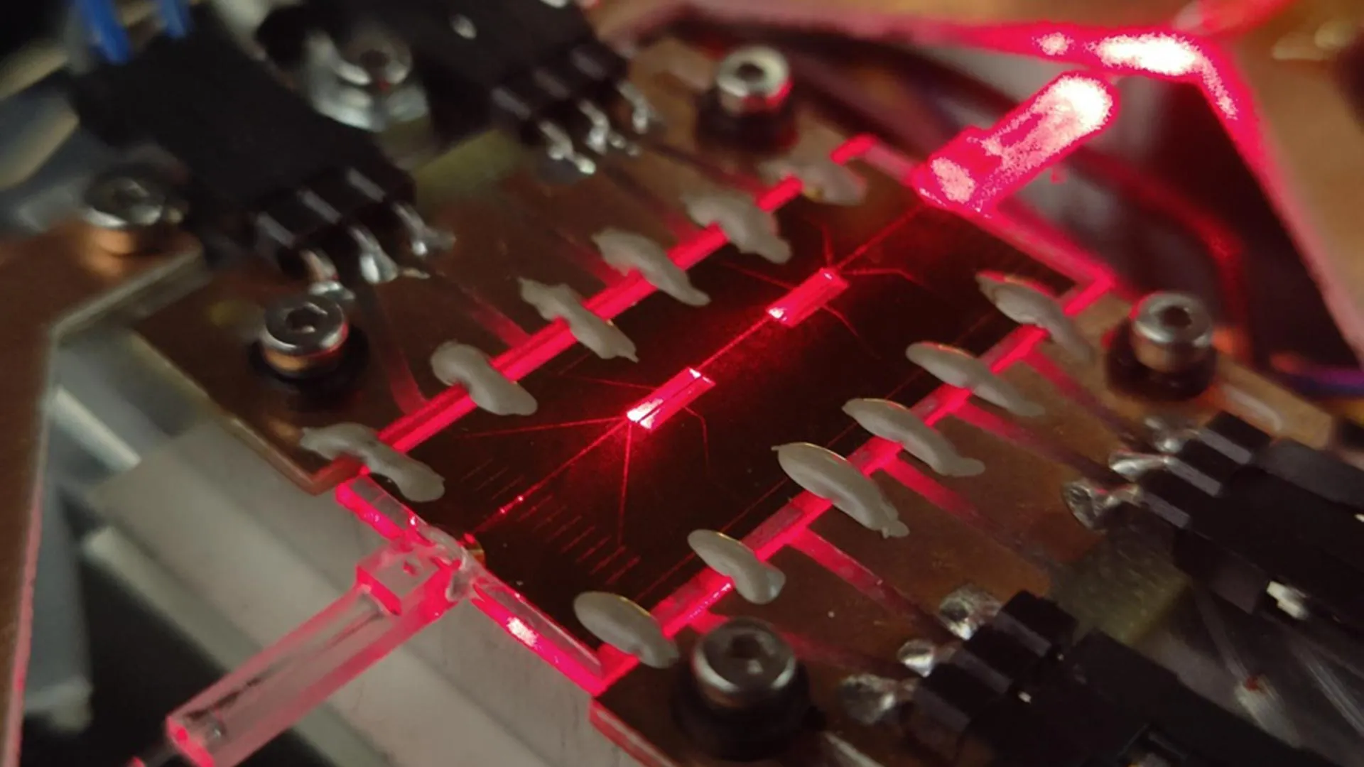
Precision Engineering: Femtosecond Laser Micromachining
The ability to harness the intrinsic advantages of glass for integrated quantum photonics relies heavily on advanced fabrication techniques. Femtosecond Laser Micromachining (FLM) is the enabling technology behind this innovation. This highly precise method utilizes ultrashashort laser pulses (on the order of femtoseconds, 10⁻¹⁵ seconds) to induce localized, permanent modifications within the bulk of transparent materials like glass.
The process works through non-linear absorption: the intense electric field of the femtosecond laser pulse causes multi-photon absorption in the glass, leading to highly localized energy deposition. This energy creates a micro-plasma, which, upon cooling, results in a permanent change in the material’s refractive index. By precisely controlling the laser’s position and intensity, researchers can "write" optical waveguides and other photonic structures directly inside the glass, forming complex three-dimensional circuits with exquisite accuracy.
This direct-write approach offers unparalleled flexibility in designing and prototyping photonic devices. Unlike traditional semiconductor manufacturing, which involves multiple lithographic and etching steps on a surface, FLM allows for the creation of intricate light-guiding paths deep within the material. This capability is pivotal for realizing compact, low-loss interferometers and couplers essential for quantum coherent receivers. The precision of FLM ensures minimal scattering and propagation losses, which are critical for preserving the delicate quantum states of light. This technique thus transforms a simple block of glass into a sophisticated quantum optical laboratory on a chip.
The Architecture of a Quantum Coherent Receiver in Glass
The core of this innovation is a fully tunable heterodyne receiver, meticulously crafted within the borosilicate glass using FLM. In the realm of Continuous Variable (CV) quantum information, a heterodyne receiver is a crucial component for measuring the amplitude and phase (known as "quadratures") of a quantum light field. Unlike Discrete Variable (DV) approaches that measure individual photons, CV methods encode information in the continuous properties of the electromagnetic field, requiring precise measurement of these quadratures.
The integrated glass chip is designed to combine a weak incoming quantum signal with a stronger, well-characterized reference beam, known as a local oscillator. This combination occurs via integrated directional couplers or beam splitters, which are precisely formed by the laser-written waveguides. The interference pattern generated by this combination carries information about the quantum state of the signal. The "tunability" of the device, likely achieved through integrated thermo-optic or electro-optic phase shifters (or precise control of the local oscillator), allows for active adjustment of the relative phase between the signal and reference beams, which is essential for accurate quadrature measurement and calibration.
The chip’s architecture enables the simultaneous measurement of two conjugate quadratures – typically the amplitude and phase quadratures. This is accomplished by directing the interfering beams to balanced photodetectors (which may be integrated or hybridized onto the chip). The ability to measure these quadratures simultaneously and with high fidelity is fundamental for reconstructing the full quantum state, thereby enabling advanced CV-QKD protocols and robust QRNG. The inherent low optical loss of the glass waveguides and the device’s exceptional stability contribute significantly to maintaining the delicate quantum coherence of the signals throughout the measurement process, a prerequisite for high-performance quantum communication.
Unprecedented Performance for Quantum Security Applications
The glass-integrated quantum coherent receiver has demonstrated performance metrics that not only match but often surpass those of existing silicon-based photonic receivers, opening new avenues for practical quantum security.
For Quantum Random Number Generation (QRNG), the device achieved a record-high secure random bit generation rate of 42.7 Gbit/s. True randomness is an indispensable resource for all cryptographic applications, from key generation to protocol initialization. The "source-device-independent" nature of the QRNG system demonstrated is particularly significant. It means that the security of the generated random numbers does not depend on trusting the internal workings of the optical source producing the quantum signals. This robustness against potential device imperfections or malicious tampering significantly enhances the practical utility and trustworthiness of the random number generator. Such high rates combined with enhanced security represent a significant leap forward in providing the cryptographic community with an abundant supply of truly unpredictable randomness.
The same versatile chip was also successfully employed for Continuous Variable Quantum Key Distribution (CV-QKD) using a QPSK (Quadrature Phase-Shift Keying) encoding protocol. In CV-QKD, information is encoded not in single photons but in the quadratures of coherent light states. QPSK involves encoding information onto one of four distinct phase states within a quantum constellation, allowing for higher information density per quantum state. In a simulated 9.3-kilometer fiber link, the system achieved a secure key rate of 3.2 Mbit/s. This performance underscores the potential for glass-based integrated photonics to support advanced CV-QKD protocols, overcoming the limitations of polarization sensitivity and higher losses often associated with silicon platforms. The ability to perform both high-speed QRNG and secure QKD on a single, compact chip highlights the remarkable versatility and efficiency of this glass-based photonic front end.
The Path to Industrial Scale and Real-World Deployment
Beyond its impressive technical performance, the use of glass in integrated quantum photonics offers several compelling practical advantages that are critical for transitioning quantum technologies from the laboratory to widespread industrial and commercial deployment.
Robustness and Durability: Glass is inherently a robust material. Its chemical inertness means it is resistant to corrosion and degradation, ensuring long-term operational stability. It also exhibits excellent mechanical strength and thermal stability, making devices resilient to environmental fluctuations such as temperature changes and vibrations. This durability is paramount for applications in harsh environments, including industrial settings, outdoor installations, and even the demanding conditions of space-based quantum communication systems, where radiation hardness is also a crucial factor.
Cost-Effectiveness and Scalability: While femtosecond laser micromachining is a high-precision technique, the raw material (borosilicate glass) is abundant and inexpensive. Compared to the multi-billion-dollar fabrication facilities required for advanced semiconductor manufacturing, FLM offers a more flexible and potentially lower-cost path to manufacturing complex photonic circuits, especially for niche quantum applications. The ability to rapidly prototype and iterate designs also contributes to overall development efficiency.
Integration with Existing Infrastructure: A key advantage of this glass-based approach is its intrinsic compatibility with existing fiber optic communication networks. Quantum signals can be transmitted over standard optical fibers, allowing for seamless integration into current telecommunications infrastructure without requiring a complete overhaul. This compatibility significantly reduces the cost and complexity of deploying quantum communication systems, facilitating their adoption in real-world scenarios.
Long-Term Reliability: For critical infrastructure applications, such as securing financial transactions, government communications, or power grids, devices must operate reliably for many years. The inherent stability and durability of glass-based photonic circuits ensure a long operational lifespan with minimal degradation, providing a trustworthy foundation for future quantum networks.
Future Trajectories and the Quantum Network Ecosystem
The development of high-performance quantum coherent receivers in laser-written glass represents a pivotal step toward building a global quantum internet. The versatility of this platform extends beyond QKD and QRNG, with potential implications for other nascent quantum technologies, including quantum sensing, quantum metrology, and even components for future quantum repeaters necessary to extend quantum communication distances.
The next phases of research will likely focus on further increasing the integration density, potentially incorporating other active components like photodetectors and light sources directly onto or alongside the glass chip through hybrid integration techniques. Further optimization of optical losses, enhancement of tunability, and the development of robust packaging solutions will be critical for commercialization. Standardization efforts will also play a crucial role in ensuring interoperability between different quantum devices and networks.
This work highlights glass-based integrated photonics as a durable, versatile, and cost-effective platform poised to bridge the gap between experimental quantum setups and deployable quantum networks. By leveraging these advantages, the technology could help accelerate the transition of quantum communication from controlled laboratory environments to real-world infrastructure, fundamentally enhancing cybersecurity for critical sectors worldwide. This strategic advancement underscores the ongoing global race for quantum technological leadership, positioning glass as an unexpected yet powerful contender in the future of secure information exchange.